- 您现在的位置:买卖IC网 > Sheet目录114587 > 550AD669M327BGR (SILICON LABORATORIES) VCXO, CLOCK, 669.327 MHz, LVPECL OUTPUT
Si550
Rev. 0.5
5
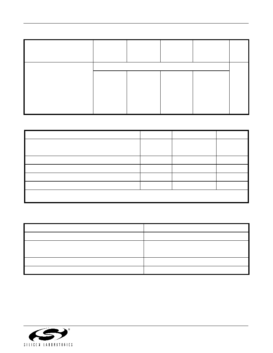
Table 7. CLK± Output Phase Noise (Typical)
Configuration
fC
KV
Output
74.25 MHz
45 ppm/V
CMOS
300 MHz
90 ppm/V
LVPECL
622.08 MHz
45 ppm/V
LVPECL
Units
Offset Frequency (f)
100 Hz
1kHz
10 kHz
100 kHz
1MHz
10 MHz
100 MHz
L (f)
dBc/Hz
–94
–117
–128
–135
–138
–143
n/a
–74
–98
–112
–122
–134
–144
–147
–77
–101
–114
–118
–128
–144
–147
Table 8. Absolute Maximum Ratings
Parameter
Symbol
Rating
Units
Supply Voltage
VDD
–0.5 to +3.8
Volts
Input Voltage
VI
–0.5 to VDD + 0.3
Volts
Storage Temperature
TS
–55 to +125
C
ESD Sensitivity (HBM, per JESD22-A114)
ESD
>2500
Volts
Soldering Temperature (lead-free profile)
TPEAK
260
C
Soldering Temperature Time @ TPEAK (lead-free profile)
tP
10
seconds
Note: Stresses beyond those listed in Absolute Maximum Ratings may cause permanent damage to the device. Functional
operation or specification compliance is not implied at these conditions.
Table 9. Environmental Compliance
The Si550 meets the following qualification test requirements.
Parameter
Conditions/ Test Method
Mechanical Shock
MIL-STD-883F, Method 2002.3 B
Mechanical Vibration
MIL-STD-883F, Method 2007.3 A
Solderability
MIL-STD-883F, Method 203.8
Gross & Fine Leak
MIL-STD-883F, Method 1014.7
Resistance to Solvents
MIL-STD-883F, Method 2016
发布紧急采购,3分钟左右您将得到回复。
相关PDF资料
552AC000189BGR
VCXO, CLOCK, 126.2 MHz, LVPECL OUTPUT
554CD000010BGR
VCXO, CLOCK, 108 MHz, CMOS OUTPUT
554CD000110BGR
VCXO, CLOCK, 108 MHz, CMOS OUTPUT
550AD216M000BGR
VCXO, CLOCK, 216 MHz, LVPECL OUTPUT
554MD000244BG
VCXO, CLOCK, 166.6286 MHz, LVPECL OUTPUT
550BF54M0000BG
VCXO, CLOCK, 54 MHz, LVDS OUTPUT
550CC25M0000BG
VCXO, CLOCK, 25 MHz, CMOS OUTPUT
550DD1046M00BG
VCXO, CLOCK, 1046 MHz, CMOS/TTL OUTPUT
相关代理商/技术参数
550AD669M327DG
制造商:Silicon Laboratories Inc 功能描述:CNTRLD OSC 669.327MHZ VCXO LVPECL 6SMD - Trays
550AD669M327DGR
制造商:Silicon Laboratories Inc 功能描述:
550AD74M1758DG
制造商:Silicon Laboratories Inc 功能描述:OSCILLATOR - Trays
550AD75M1758DG
制造商:Silicon Laboratories Inc 功能描述:OSCILLATOR - Trays
550AD77M7600DG
制造商:Silicon Laboratories Inc 功能描述:CNTRLD OSC 77.76MHZ VCXO LVPECL 6SMD - Trays
550AD983M040DG
功能描述:VCXO振荡器 SINGLE VCXO 6 PIN 0.5PS RS JTR RoHS:否 制造商:Fox 封装 / 箱体:5 mm x 3.2 mm 频率:19.2 Mhz 频率稳定性:2.5 PPM 输出格式: 封装:Reel 电源电压:3 V 端接类型:SMD/SMT 尺寸:3.2 mm W x 5 mm L x 1.5 mm H 最小工作温度:- 20 C 最大工作温度:+ 75 C
550AE000131DGR
制造商:Silicon Laboratories Inc 功能描述:CNTRLD OSC 669.32658MHZ VCXO LVPECL 6SMD - Tape and Reel
550AE100M000DG
功能描述:VCXO振荡器 550 VCXO LVPECL 3.3V 100MHz RoHS:否 制造商:Fox 封装 / 箱体:5 mm x 3.2 mm 频率:19.2 Mhz 频率稳定性:2.5 PPM 输出格式: 封装:Reel 电源电压:3 V 端接类型:SMD/SMT 尺寸:3.2 mm W x 5 mm L x 1.5 mm H 最小工作温度:- 20 C 最大工作温度:+ 75 C